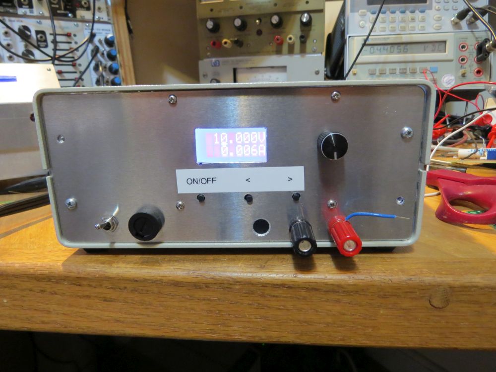
PS-Load Page
Power Supply / Load or
2/4 quadrant voltage current source / meter
Arduino-based Power Supply / Load
The Schematics, PCB files,
and Simulation models are here
Here is the DIY-SMU
project
 As an EE, I have designed, used and messed with power
supplies for much of my life. My Power-One blog attests to this.
As part of this work I have built a number of load circuits from
arrays of power resistors to a simple electronic load, to a
combined power supply and load circuit. As Keithley and Hewlett
Packard and others long ago discovered, a combined power supply
and load has some advantages. It combines the functions of a power
supply, an electronic load, a voltmeter, and a current meter. As a
result it can fully test batteries, solar panels, power supplies,
or any power source. When testing batteries, it can charge or
discharge using any type of charge cycles. So it is great for
battery research and testing. It can either test or simulate a
battery. It can test high power LEDs, or other semiconductor
devices, and provide V-I curves, similar to a semiconductor curve
tracer. An when not providing these advanced functions, can be
used as just another lab power supply.
As an EE, I have designed, used and messed with power
supplies for much of my life. My Power-One blog attests to this.
As part of this work I have built a number of load circuits from
arrays of power resistors to a simple electronic load, to a
combined power supply and load circuit. As Keithley and Hewlett
Packard and others long ago discovered, a combined power supply
and load has some advantages. It combines the functions of a power
supply, an electronic load, a voltmeter, and a current meter. As a
result it can fully test batteries, solar panels, power supplies,
or any power source. When testing batteries, it can charge or
discharge using any type of charge cycles. So it is great for
battery research and testing. It can either test or simulate a
battery. It can test high power LEDs, or other semiconductor
devices, and provide V-I curves, similar to a semiconductor curve
tracer. An when not providing these advanced functions, can be
used as just another lab power supply.
What is the difference between a source-meter and a lab Power
Supply? Both can source current and voltage, and measure current
and voltage, making them one quadrant devices. The difference is
that generally a source-meter is a four quadrant device. I will
show that a 2 quadrant device that contains a positive source or
load can be a useful configuration. The number of
"quadrants" refers to the polarity of the output voltages and
currents, as shown in this diagram.
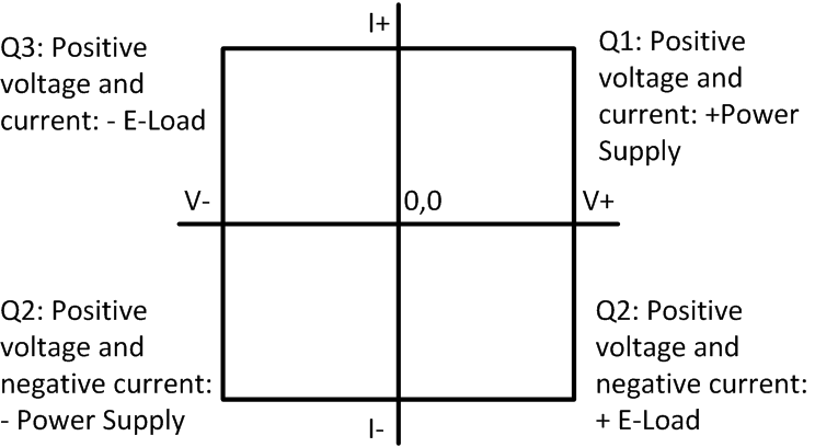
But only a few power specialized power supplies can sink current.
the HP6632A and its siblings are examples of power supplies that
can provide a load. Seems like a useful thing to have.
Particularly since it only costs a few extra components and a bit
more control circuitry over a simple power supply.
To generate a negative power supply, one typically connects a
positive supply in reverse, with its + terminal to common (ground)
Then it is still a one quadrant device, but a different quadrant.
A source-meter can typically provide both + or - voltages, and can
source or sink (+ or -) current while providing either polarity
voltage. They are therefore 4 quadrant devices. A source-meter
that can only do positive voltage but can source and sink current
is a 'two quadrant' device. For testing semiconductor
devices, four quadrants is almost a necessity. However, there are
advantages to 2 quadrant devices which I discuss below.
A few years back, I built a simple 2 quadrant VI which is
described in the Power One page. I have used this to test high
power LEDs and batteries. However, this circuit has some
limitations. For one, it did not have front panel controls, so it
always requires a PC to control it. If the PC crashes or the power
goes out during your battery test, you lose data and worse, can
over-charge or discharge the battery, causing damage and possibly
a fire. Also most power supplies are not designed to drive a
battery. If you inadvertently power the supply down, the supply
may be damaged by having a high-current voltage on it's output. It
is important that any battery teste power down gracefully if the
AC is removed.
Keithley source-meters are fine precision devices with multiple
current ranges allowing them to source and measure currents from
Amps down to microcroamps, and below. They use 5 digit meter
circuits, and are generally four quadrant devices. As a result,
you pay for these capabilities, typically $4000 for a single
channel 2400 unit. If you need to test multiple batteries
simultaneously, which is often the case as it takes a long
time to charge or discharge a battery, this gets expensive fast.
For a programmable lab power supply, ADC and DACs are needed,
current and voltage measure circuits, a series pass power element
(transistor plus heat sink). What I propose here is a combined
power supply load that is flexible and accurate enough to perform
a range of test functions, and that has the following
capabilities:
- Nominally 2
quadrant, 0 to +24V
- Optional -24V (4
quadrant)
- 0 to 3 Amp Source
- 0 to 5 Amp Sink
- Vset resolution
about 10mV
- I+ and I- set
resolution about 10mA
- Vmeasure resolution
to 1mV
- Imeasure resolution
to 1mA
- 0.1% or better
overall accuracy
- Full isolation from
ground
System and Packaging:
- Single CPU and front
panel can control 1 or up to 4 isolated channels on one I2C
bus
- Each of the 4
boards supports different I2C addresses
- Boards can use any
Arduino, Raspberry Pi, or any other CPU for control
- Multiple channels
can be packaged together
- Single shared
supply (lower cost, common ground)
- Or separate
supplies (isolated ground)
- Fan control,
variable speed
- For raw power, can
use transformer / rectifier / filter or low-cost switching
supply
For controls, an optional
Front Panel board provides:
- Arduino Leonardo
Compatibility
- 16x2 or 8x2
LCD, large or small
- 4.5 digit display
for currents and voltages
- Encoder knob for
setting voltages and currents
- LEDs for status on
each supply
- USB control from PC
- Controls and PC
isolated from power
A programmable lab supply
is one with an external interface such as GPIB or USB. It uses the
same basic power and control circuits, but instead of using
potentiometers to set voltage and current, it uses DACs, and
instead of a digital panel meter to read current and voltage, it
uses an ADC. Once a supply is programmable, adding a front-panel
consisting of a simple processor, display and controls is
straightforward. Ideally a single front panel can control and
multiple supplies with a simple menu system.
The other elements of a programmable power supply are a raw DC
supply, some low voltage DC supplies for the control circuit, a
series pass element and its thermal management (heat sink, fan),
control circuitry, a crossover capable of smoothly switching
between constant current and voltage control, a reference voltage,
and current and voltage measuring circuits. Typically there is a
turn-on circuit and status LEDs that indicate whether a channel is
on, and in constant current or voltage mode.
To make a 2 quadrant PS-Load, a second series pass element is
required. Since only one series pass element is drawing current
and therefore dissipating power at a time, it can share the heat
sink and fan with the other device. Another DAC to set the
negative current is optional. My original 2 quadrant design used a
single DAC to set the + and - currents to the same value but
opposite polarity with good successes. Some commercial products
also use this shortcut.
To make a 4 quadrant device, the raw supply provides both + and -
voltages. The advantage of 4 quadrants is that it can provide
either + or - voltage under user control. A disadvantage is that
it may be easier to fry a DUT by inadvertently applying a negative
supply. A subtle but important downside of a 4 quadrant system is
that when using it as a load, the current for the load is
generally derived from the negative supply, not the ground return.
The negative pass element therefore has the negative raw
supply voltage plus the positive load voltage across it. This
burns much more power than a normal electronic load, or a 2
quadrant device where the negative pass element is simply
grounded. So the circuit tends to be power limited instead of
current limited, and therefore cannot sink as much current.
So if you plan to use your PS-Load as a high power load such as a
battery or power supply tester, the 2 quadrant version is
preferable, and also slightly lower cost.
Output Stage
There are many output
stage designs that can be used including bipolar transistors and
FETs. Here are the general output stage requirements:
- Low impedance output
for stability into different loads
- Able to shut
off using software or hardware commands
- Able to shut off if
power is not applied: powers down to a benign condition
- Able to go to low
voltage as a load: less than 1V at full current
Emitter followers using
bipolar transistors can meet most needs except for the low voltage
requirement. FETs can achieve < .1 ohm to GND as a load.
Complimentary, common-drain MOSFETs can pull the supply very close
to the rails (low drop-out), but have a high output impedance
(essentially a current source) until they come close to
saturation. This high impedance means that the amplifier loop gain
is a strong function of both the load resistance and capacitance.
This makes it difficult to stabilize the loop for all kinds of
loads when these types of stages are used.
Complimentary Source followers have low output impedance, but
require gate drive circuits that exceed the power supplies, or
else can have up to 5V loss at high currents. I call the high
voltage supplies V++ and V-- boost supplies. These can be built
with a simple charge pump consisting of a 555 oscillator and some
diodes and capacitors. This type of stage requires that the driver
amplifier have a fairly high power supply voltage rating: the raw
supply (+/- 25V) plus about 12V extra on each supply is 74V. There
are several amplifiers that meet this need. To accommodate even
higher supply voltages or unregulated supplies, the supply
requirements are higher. Linear has a nice high-voltage opamp,
LTC6090 that accommodates up to 140VDC and costs about $3 (q100).
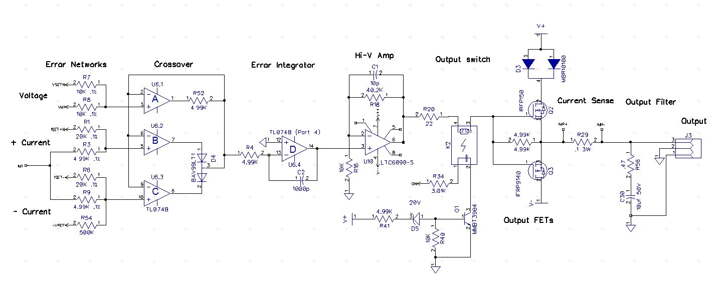
Simplified Control and output circuit for single
quadrant (+24V) version: The shut-off integrator
control circuit is not shown here.
My initial spec of +/- 24V output range can be met with a +/- 25V
power supply. These can be met with low-cost 24V switchers
adjusted to 25VDC. This allows 0.5V drop for the current shunt and
0.5V for the FET, wiring, and fuse. Figure 0.25V at 5A for the
FET, or 50 milliohms.
This type of output stage is quite simple. Both FET's gate pins
are tied together, and both source pins are connected. A single
resistor from both Gates to both Sources will turn off both FETs.
Apply a positive voltage and the + NFET turns on. Apply a negative
voltage and the - turns on. Another advantage is to use a simple
passive switch between the voltage amplifier stage and the FET
gates to turn OFF the output stage.
This type of output works well when one FET is on and when the
load changes quantity. But in the case when the load current
changes polarity, the output stage takes a few hundred uS for the
drive voltage to change the few volts from turning on one FET to
turning on the other. In an audio amplifier, this load current
polarity change occurs on every cycle of AC, and would cause
horrid crossover distortion. In the case of a Voltage / current
source, it occurs rarely and the circuit recovers quickly.
Crossover Design:
Single integrator
Crossover design refers
to the current and voltage control circuitry. It is called a
crossover because it must cleanly switch from voltage to current
control and vice versa. There are a lot of ways to implement this.
Most basic power supplies use two integrators, one for voltage and
one for current. Then diode logic is used to control the pass
element with current control taking priority over voltage control.
The disadvantage of this type of control is that when the loop is
regulating in one mode, the other integrator goes to its maximum
output. Then when the load or setting is changed and the other
integrator takes control, the output voltage or current can
overshoot while waiting for the other integrator to slew to the
correct value. Overshoot is generally bad in a power supply. This
problem only gets worse with a 2 or four quadrant device. A third
integrator is required for the load side (quadrant 2) or -current
control.
The approach I took uses a single integrator with active diode
logic to select the error voltage from either the voltage,
+current, and - current sources. There are three error amplifiers
each consisting of a basic op-amp plus a diode. These slew quite
fast to control the single integrator and so overshoot is
minimized.
Power-Off Circuit
If you analyze the
circuit of a typical power supply, you will see that things get
complicated if you apply an external power supply (battery) and
then turn off the supply. I have toasted a couple of power
supplies doing this, and since I want this PS-Load to be able to
test batteries and other sources, I designed it from the start to
be able to handle this condition gracefully.
To turn off the supply, the output stage must be somehow disabled.
with a simple load, simply setting the output to 0.0V may be
adequate. But when the load is another voltage source, the output
current must be reduced to zero. The complimentary FET
output stage does this nicely, with the single gate resistor
nicely turning off both FETs. But it is necessary to somehow
isolate the gates from the driving amplifier. I chose a
Photomos(TM) FET switch for this function. These $1 devices have
the advantage of requiring no power supply pins, and so to turn
them off, simply do not drive the LED input. So when the power
supply is off, the FET is guaranteed to be off. Perfect. A relay
would also provide this function. The Photomos devices are smaller
and never wear out. The typically switch in about 1mS and handle
milliamps up to amps, and will switch 100 or more volts.
But when the Photomos is turned off, what about the integrator?
The control loop is now broken, so the integrator will slew to one
extreme or the other. Then when you turn the switch back on, the
output voltage will have a huge glitch. You could reset the
integrator to 0V, but if the load is a 12V battery, the turn-on
current transient will be huge until the loop recovers. Not good.
One solution, used by HP in their excellent HP6632A supplies, is
when the output is OFF, to control the integrator to output the
same voltage that the output pin is. For example, if the output is
a 12V battery, the output of the integrator and driver op-amp is
controlled at 12V. Then when the Photomos is turned back on, the
FETs have no gate voltage and are initially off. This elegant
solution works very well both in simulation and in reality.
The Turn-On/Off circuit
has a few requirements. When PS-Load is OFF, I want the OFF
current to be as low as possible, preferably just a few uA. I like
the nice simple approach of using complimentary FETS as output
stages, with a simple resistor to bias them OFF. This requires
some isolation from the voltage amp when in the OFF state. I use a
Photomos solid-state relay. If you haven't used these, they are
pretty cool for low and medium current switching. They are
optically isolated and consist of an LED plus MOSFET switches.
They have on-resistances in the 50 down to 0.1 ohm range, can
output AC or DC switch voltages up to 100's of volts, and provide
thousands of volts of isolation from the LED to the switch. They
are available from a handful of manufacturers and with safety
ratings for AC line applications. They are like a relay but use
less voltage and current to drive: 1.2V at a few milliamps. They
are more reliable than relays with no moving parts or contacts to
wear out. They are small in a 4 pin SO or DIP package, and cheap,
about $1. Like a relay they do not turn on or off instantly, but
take about 1 millisecond, similar to a reed relay. Larger armature
relays take 10s of milliseconds. So one of these is used to
connect / disconnect the voltage amp to the FET gates.
When the circuit turns ON, the output voltage should slew cleanly
from its idle voltage to the voltage setting. For example, imagine
a 12V battery connected to the output. When the output is OFF, I
want minimum load on the battery. When the supply goes ON, I want
minimum transient current to occur. When OFF, the output FET gates
are held at the output voltage by the bias resistor. But when ON,
the gate voltage is switched to the high voltage amp output
voltage. If that voltage was for example 12V, this would turn ON
the P-Fet hard for a few milliseconds until the current and
voltage loops could take over. Turning a FET on hard between
Ground and a 12V battery can toast it due to the extremely high
instantaneous current. Hopefully the output fuse would blow before
the FET, but nuisance fuse blowing is also bad.
The fix for this problem is to hold the high voltage buffer amp
output near the supply output voltage when the supply is OFF. Then
when the Photomos is turned ON, the gates and sources of both FETs
are at the same voltage, and the FETs are initially OFF. A
separate voltage divider measures the buffer amp voltage and
compares it to the Output voltage. This error signal. Vbuf - Vout
controls the integrator when the supply is OFF, holding the buffer
at the output voltage. A CMOS switch, DG419, switches the
integrator input between normal operation and this difference
signal. A logic signal called ON from the I2C bus, controls this
CMOS switch and also turns on the Photomos.
I finally got a nice digital scope and can now measure power
supply transient behavior. When I hit the ON button, with PS-Load
set to 5.0V, I saw a nasty +15V transient for about 300uS.
Definitely bad power supply behavior. When the ON signal goes ON,
two things occur. The integrator is switched from the voltage amp
to the to the error amps, and the output stage is connected to the
voltage amp. But the DG419 switch for the integrator switches in a
few nS, while the Photomos switch takes about 500uS to turn on. So
the integrator starts slewing right away, but the loop is broken
for 500uS. The fix is to make the integrator control input (DG419)
as slow as the Photomos. So I added a 500uS RC delay to the DG419
control signal.
Speaking of Simulation
I generated an LTSpice
simulation for this design. Do not underestimate the complexity of
a lab power supply. They must remain stable over a wide range of
resistive and capacitive loads, and must switch from constant
voltage to constant current cleanly and without overshoot.
Designing and testing circuits for all of these conditions is
work. It is much easier to test them with a simulator and observe
the step response. Then when the simulation performs well, build
and test a real circuit.
Current Sense: Many
possible configurations
High side or low side
current sense? High side means that the current sense resistor is
in series with the + output of the supply. Low side means it is in
series with the ground. High side is required if you have multiple
supplies operating from the same raw supply. Low side is simpler
since the sense amp doesn't need to deal with common mode voltage
changes.
With the hundreds of current sense ICs on the market, this should
be easy, no? No. All current sense chips require a minimum voltage
of a few volts to operate. With a lab supply where the output
voltage can be 0V, they won't work without tricks. And forget
about measuring current when the voltage is negative. So they
don't work for either high side or low side applications.
With a high side current sense amp, common mode is an issue. Take
a typical application:a 0 to 25V power supply with a .1 ohm 5A
current sense. 5A is 0.5V across the sense R, and if you want
about 1mA accuracy, that is 100uV across the R. If the voltage can
be 0 to 25V, and you don't want the current reading to change more
than 1mA, that is 25V / 100uV = 250,000 :1 or 108 dB Common mode
rejection ratio (CMRR). Yikes! Some instrumentation amplifiers can
do this, but the problem is that the amplifiers require high
voltage power supplies. If you use a resistive differential amp,
the resistor matching is from hell. You can trim the CMRR with a
trimpot, but 250:000:1 is tough. Normal 1% resistors are spec'ed
at 100ppm drift per degree Celsius. 1/250,000 is 4ppm total drift
over the full temperature range.
I used a compromise: 25ppm 0.1% resistors (available for about
$.20) and a nice 20 turn trimpot. The circuit works quite well but
is not designed to hold that CMRR across a wide temperature range.
I2C
In the inevitable
discussion between I2C and SPI, there are many trade offs. I
generally choose I2C where speed can be slow, and isolation, and
multiple addresses (devices) are required. So for a fast
ADC, use SPI, but for this relatively slow Sigma-Delta
ADC, I2C is fine. I need DACs, a multi-input ADC, general
purpose IO (GPIO) and an EEPROM to store setting and calibration
data. In addition, I might use 3 or 4 identical PS-Load boards
in a system with a single processor controlling it all. So one
parameter I looked for in selecting the I2C peripherals was the
ability to easily select 4 I2C addresses per each device.
Isolation
A system power supply needs to
be isolated from the computer system that is controlling it.
Imagine a USB interface to a non-isolated power supply, and the
operator accidentally shorts the 24V 3A output to ground. That
will cause 3A to flow through the AC ground pin, or worse, the ground pin of the USB cable to the PC. Not good.
For this and other reasons, isolation is needed.
I2C isolation is a bit tricky since at least the Data wire needs
to be bi-directional. For multiple masters (rare) the clock would
also be bidirectional. Fortunately there are I2C specific
isolators that address this trickiness. I use the ISO1541 from TI
in a SO8 package for about $4.
Power Supplies
The system can use any raw
power supply including low-cost switchers, and conventional
transformer / diode / caps. To generate 24V, I use a
low-cost 24V switcher set to +25.5V so the supply can output 24V
at full current, including wiring, shunt resistor and FET losses.
In addition to the raw supply, the FETs need "boost" supplies. I
discussed these earlier.
In addition to these, the analog circuits need +/- 12V for the
analog stuff, +5V for the I2C stuff, and an isolated +5V for
the control processor.
For +/- 12V, I use a low-cost DC-DC from CUI. The 5V is a fairly
low current (a few milliamps) so I use a 5V linear regulator from
the +12V. For the isolated 5V to drive the processor, I use a
small, isolated DC-DC. Note that any isolated 5V supply can
be used. In fact if multiple channels are used, only one isolated
5V is required. and so channels 2 though 4 should not have the 5V
DC-DC installed.
ADC
After using the
Microchip16/18 bit 4 channel Sigma-Delta ADCs (MCP34xx) on
previous projects, I chose it for the ADC on this project. 16 bits
at 7.5 samples per second, but the cool feature is the ability to
measure +/- 256mV with a single +5V supply. Bipolar current and
voltage measurements need bipolar measurements. The part only uses
an internal reference, and doesn't bring it out as a pin, but it's
15ppm/C drift is quite good. I only use 2 of the 4 channels in
this design, but the 2 channel parts don't have I2C addresses, so
I use the 4 channel part here.
DACs
DAC INL (Integral
Non-linearaity) is a critical spec for a programmable voltage
source. It directly affects the accuracy of voltage and current
settings. It is important to get an accurate value when you
request it. Offset and gain errors can be calibrated out, but to
get accurate values at all settings, low INL is needed. Many
system power supplies use expensive14 or 16 bit DACs for this
purpose. I need 2 or 3 channels, one for Voltage, one for Positive
current, and one for negative current. I need 12 or more bits with
good INL, and low cost. Unfortunately most low-cost 12 bit bit
DACs have high INL, like 4-12 LSBs. 12 or more LSBs of INL is
equivalent to an 8 or 9 bit DAC. I found the Maxim MAX5815 quad 12
bit DAC that has +/-1LSB of INL Max. and is about $5. Yes, it has
address select pins. And they throw in a sweet 10ppm/C
reference. I use it for the other circuits that need a stable
voltage.
Another way to get better INL is to use the more accurate and
higher resolution ADC as feedback, and adjust the DAC setting.
With this approach, the initial setting will have the full DAC INL
error, but then the ADC corrects it. This causes a somewhat
strange settling response as the firmware control loop hunts for
the best DAC setting. I'm not sure this is an acceptable behavior.
Calibration
There is an I2C EEPROM
per channel that will ultimately contain the calibration factors
for that channel. But implementing proper cal firmware and EEPROM
storage is a lot of work, which I have not done yet. For now, I
simply hard-code the cal factors in the Arduino firmware. Since I
currently only have 2 boards built, this is a reasonable approach.
For each board, there is a table like this:
#ifdef BOARD1
Set[DVS].range_max = 25.0;
Set[DVS].set_max = 25.0;
Set[DVS].range_min = 0.0;
Set[DIP].range_max = 5.0;
Set[DIP].set_max = 3.0;
Set[DIP].range_min = 0.0;
Set[DIN].range_max = 5.0;
Set[DIN].set_max = 5.0;
Set[DIN].range_min = 0.0;
// Offset and Gain for all ADCs and DACs
Set[DVS].gain_cal = 0.939145;
Set[DVS].offs_cal = -0.022;
Set[DIP].gain_cal = 0.99475;
Set[DIP].offs_cal = -0.022;
Set[DIN].gain_cal = 1.00000;
Set[DIN].offs_cal = 0.0000;
Measure[VM].offs_cal = 0.004;
Measure[VM].gain_cal = 0.99534;
Measure[IM].offs_cal = -0.011;
Measure[IM].gain_cal = 0.99161;
Measure[VM].range_max = 13.00;
// 2Q: /13 only
Measure[IM].range_max = 20.0;
// .1 ohm = 10V/A
Set[DIP].value = 3.000;
// Set initial current values
Set[DIN].value = 3.000;
#endif
To begin calibration, I set the offsets to 0.00 and the gains to
1.00. I start by calibrating the16 bit Voltage ADC: apply 0.0V to
the output (a short or low value resistor, power supply OFF) and
see what the voltage display reads. Lets say it reads +0.015V. So
the voltage measure offset, Measure[VM].offs_cal is -0.015V.
Then set the output to about +20V and compare the measured
(display) and expected (DMM) values. Divide them, and that is what
you wold need to scale the measured by to obtain the expected.
Set Measure[VM].gain_cal to that number. Do the same for the
current readings.
Once the measure circuit is working, you can use it to measure and
calibrate the voltage DAC and two current DACs. I generally enter
the offset number and recompile before calibrating the gain. More
compiling, less thinking. The first time you do this will will
take a bit of time, but once you get the hang or it, maybe 20
minutes to calibrate everything. Notice that I got lazy and did
not cal the negative DAC [DIN] yet.
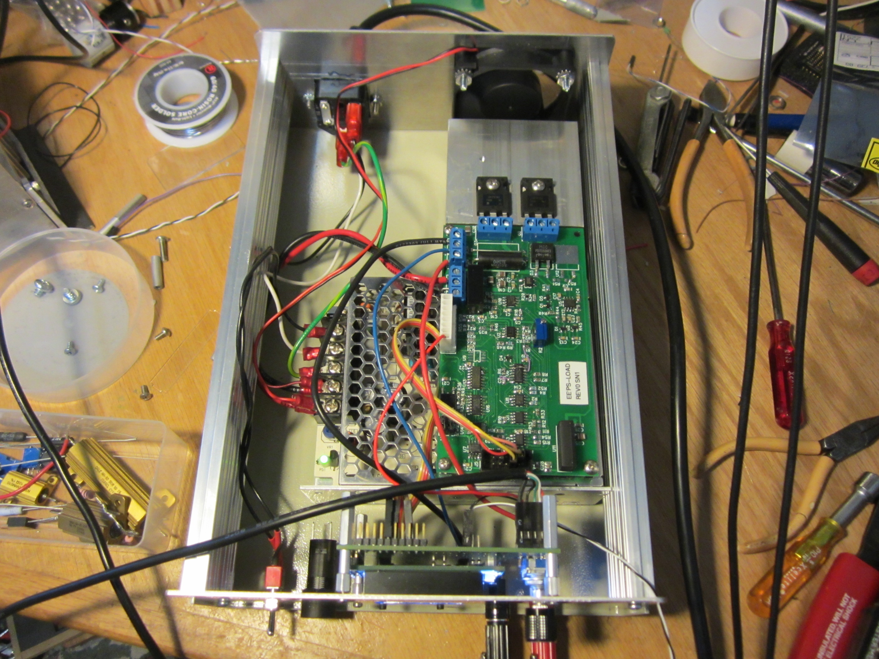
Enclosure
My goal is to minimize
the case size. I would like to fit a single channel into a
small 2U (3.5") high by 1/4 rack (4.25") wide case. Length should
be 10-12". I came across a large batch of free Hammond 1402F
enclosures. These are 7x10x3", and fairly attractive. Here is a
single channel system in a Hammond case. Note the switching supply
beneath the PS-Load board. For an AC inlet I use a fused version,
although switching supplies already have AC fuses. If the design
uses a transformer, then a fuse is required. Also since I run AC
to the front panel, an AC fuse is a good idea.
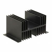
For a heat sink, I used a 2.6 x 1.5 x 2.4" one cut from a larger
heat sink I found on Ebay. It is a bit too small to dissipate
50-75W, so I currently run at a bit lower power. The 24V fan blows
air out of the enclosure, which I think is not quite as efficient
as blowing cold air directly onto the heat sink. I still have some
work to do here. Ideally I would find a larger heat sink. Note
that for two or three channels, a single wider heat sink could be
used and multiple boards could be mounted side-by-side. Currently
the height of the heat sink and the switcher are about the same,
so I just mount a couple of short spacers on the switcher to hold
the front two mounting holes of the board. It's a bit of a hack,
but it works. It requires removing the cover of the switcher to
mount the spacers, nuts, and washers. You could also just use long
spacers for the board. The switcher fits between the board
mounting holes.
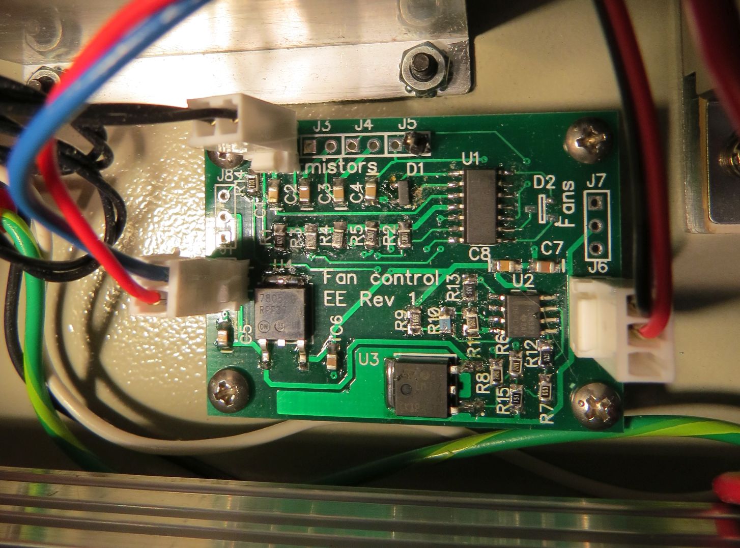
Internal view with the original heat sink and no fan board
New heat sink with thermistor and fan board installed.
The original heat sink was a bit small and did not cool
efficiently. Too much of the cooling air diverted around the heat
sink. Also it had no mounting features. I purchased another large
heat sink extrusion on Ebay, cut it to size on my trusty table
saw, and mounted it to two small angle brackets. It is raised
about .25" off the chassis bottom to allow air to flow efficiently
past it. This new one works well. Ideally there would be fins
above the heat sink as well as below it. Here is an off-the shelf
Wakefield 395-1AB that is about the right size, should work
nicely and costs about $22.
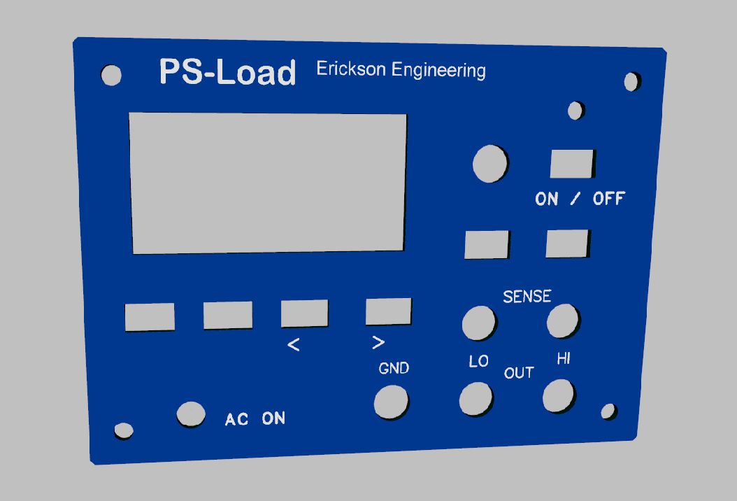
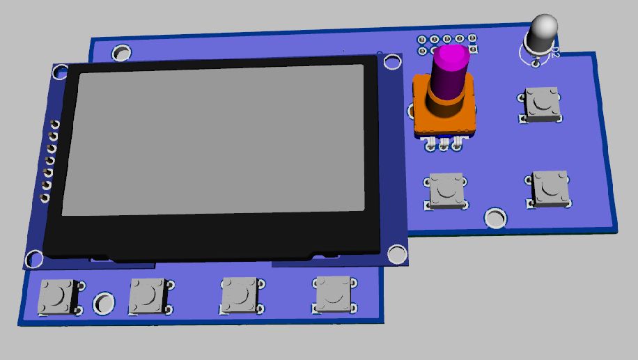
Front panel controls, Encoder, push buttons and LCD. No Green
binding post yet.
Fan Control
A thermally controlled
fan is generally good. When the supply is not outputting much
power so the heat sink is cool, the fan can be OFF. When it is
operating at max power, the fan is ON full. In the middle it wold
be nice to have th4e fan ON but quiet since no-one wants to hear a
fan that is on unnecessarily or is constantly varying in speed,
the sound is annoying and distracting. So the speed should
change only when it needs to. It's a trade-off between optimal
cooling and noise. My design is for 3 fan speeds: Off, full on,
and medium. This should do the job and minimize fan speed changes.
Most DC fans are 12V, but I have lots of 25V power and little 12V,
so use a 24V fan. But the fan controller should also accept 12V
power and drive a 12V fan. I might want to have multiple heat
sinks or a large one with multiple temp sensors. I might want to
have 2 fans. Since the 24V is electrically isolated from the CPU
or I2C control, any feedback or controls from the CPU to the fan
would need to be isolated. Fan power isolated from GND and other
supplies
- Temp detect on
multiple heat sinks 1 through 4? 2?
- Lug style
thermistors: one screw mounting, good thermal contact, no
isolation hardware required.
- Control the fan as a
function of the maximum of multiple thermistors. So maximum
logic is needed
- Alarm? 3rd
comparator, LED or audible, notify processor when a max
temperature is exceeded.
- Three settings
minimum:
- Off
< 40C, fan V < 2V
- Medium,
40-60C, fan voltage ~12V
- High:
> 60C, Fan 23V
- Hysteresis to keep
speed from varying.
I considered a few
approaches, mostly by having the Arduino control the fan. Finally
I decided that boards are cheap and I just needed a variable fan.
So I built an analog circuit that can accept 1 through 4
thermistors, drive multiple fans, and has 2 setpoints for 3 fan
speeds. Here is the schematic
and PCB. By the way, this is my first PC board order from
PCBWay.com. $10 for 5 boards, $8 shipping, 3 weeks delivery.
The maximum temperature circuit is actually a minimum voltage
circuit since high temperature on an NTC thermistor causes low
voltage. It uses a quad op-amp and 4 schottky diodes to output the
minimum of 4 thermistor voltages, representing the hottest of the
4 thermistors. I looked up the two temperature setpoints, 40C and
55C. The desired fan voltages are 0V, 12V and 23V. 12V is pretty
quiet, 23V is the maximum that the LM317 regulator can output with
a 25V input. These temperature setpoints correspond to voltages
when used with a 5V supply and a 10K bias resistor, or 1.50V and
1.25V. Then I built a simple 3 resistor chain to provide these 3
voltages. The temperature and the setpoints are compared via two
LM393 comparators, which drive resistors that set the LM317 output
voltage. Whew!
The BOM cost of the board with a single thermistor and one fan
output is about $2 plus $1 for the board. For thermistors, I use
Lug mounted. These are a bead type thermistor mounted in a copper
lug that can be mounted to a surface with a single screw. They are
about $1.
Schematic
The schematic was designed in
DipTrace. After considering the usual low-cost CAE options, I
decided on DipTrace. Unlike most CAE tools, I like it. For
years I used ExpressPCB. They were the quickest and lowest cost
way to get prototypes. But their file format is proprietary, and
many offshore vendors now produce boards much cheaper than
ExpressPCB, and require Gerber file formats. It was time to update
my skills to a real PC design tool.
I attended a Synthesizer conference at Olin College in Needham,
MA. I spoke with an EE professor there and asked him about
building prototypes for students. He said that he regularly
assigned a schematic and PCB project to students to do over a
weekend. Students who had never drawn a CAE schematic or laid out
a PC board could download and learn DipTrace quickly. When I tried
it, I was pleasantly surprised and have been using it for the past
8 months.
files/ps-load1.pdf
Costs
The BOM has costs
included. The parts on the PS-Load board are about $50, Qty 100,
pretty reasonable. In addition, A 75W 24V, 3A switching power
supply is $27. The heat sink cost is about $5-10. I buy surplus
heat sinks on Ebay and cut them to size. Then a case, 24V fan, AC
inlet, AC switch, and banana jacks.
For the front panel board, a PCB, LCD, Atmel processor, crystal,
USB connector, a couple of buttons and an encoder. I estimate $20
cost.
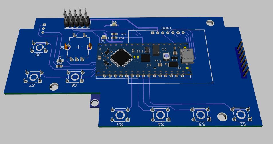
Front Panel
Board
I used the front panel
board of my Arduino Panel Meter for the processor and controls. In
addition to an Arduino Leonardo compatible (ATMega32U4) processor,
it has an 8x2 LCD, an encoder knob and positions for push button
switches. The panel Meter has isolated data acquisition circuitry
which I bypassed, and brought out its I2C circuitry. It was a good
match for this application. While the small 8x2 LCD is OK for a
single channel unit, it is a bit too small for a multi-channel
system, and the digits are fairly small. My plan it to lay out a
16x2 version that can use either a small or large digit LCD.
Firmware
I wanted to use all
Arduino code for this project to make it as accessible as
possible. I like that Arduino can do basic math in floating point
and still fit nicely in a 32KB memory. The code uses the wire
library for I2C, and the LCD library. One problem with Arduino
libraries is that they tend to use polled methods as opposed to
interrupts. I like to read front panel controls including encoders
in a 1mS or so timed interrupt routine. Fortunately the Arduino
also uses a 1mS timed interrupt using Timer0. I found a trick of
adding a second output compare to Timer0, which creates a second
interrupt. You can adjust the compare value so the second
interrupt occurs roughly halfway between the Arduino interrupts,
thus avoiding conflict. Then you can add your own code to this new
interrupt. I used this technique to create an interrupt where I
poll and debounce the keys, and to poll the encoder. Keep in mind
that this interrupt isn't exactly 1mS, but is 16Mhz / 64 /
256 = 976.5625 Hz. Arduino timer routines compensate for this
error.
Switching Power Supply
Common-Mode Noise Issue
Here is a more thorough
discussion of AC-DC and DC-DC common-mode
noise.
With any power supply, either lab or otherwise, common-mode noise
is an issue. When you float a power supply, there is always some
AC current flow from the power supply ground to the chassis (AC)
ground. With a linear supply, this is usually a small amount of
60Hz current due to the inter-winding capacitance between the
primary and secondary windings of the power transformer. With a
linear supply, the frequency (60Hz and some harmonics) and the
capacitance (50-200pF) and the 240VAC input causes about I = V /
Xc = 240/(1/2*pi*60Hz * 200pF) or tens of microamps. No problem,
and the typical .01uF safety cap to ground shunts out most of this
current. In the case of a high-class power supply or a
precision instrument, the AC transformers are usually double or
even triple shielded with metal foil between the windings. This
shielding reduces the common-mode noise current significantly.
However with a switcher and its high frequency transformer, the
frequency is not 60Hz, but the harmonics of the the fast rise-time
switching waveforms: rise times of 300V pulses can be about 100ns
causing pulses with harmonics of 10MHz or more. The transformer
windings are usually smaller, so the inter-winding capacitance is
a bit less. Just to meet radiated and conducted EMI, the
transformers are often shielded. You will sometimes see copper
foil on switching transformers.
Still, I see some pretty ugly looking common-mode switching noise
on many switchers. Manufacturers do not specify common-mode
noise, so how do you deal with it? How do you quantify it? Search
for this problem on line and you will find little specific data or
techniques. In fact, to meet EMI, Switchers are often tested with
a short and heavy wire from their DC common to the chassis ground.
This effectively shunts any common mode noise to ground. But if
your application requires a floating supply, you are on your own
dealing with this issue. Measuring the open-circuit voltage is
interesting. You will typically see a few volts of high frequency
crud. Why not 100V, since the switcher is switching hundreds of
volts? The answer is that switchers do have a capacitor from AC to
DC ground, typically between .01 -.05uF. This is a safety rated
cap in case the ground of the system is accidentally opened up.
This common mode voltage or current can shows up as noise on audio
or other critical analog circuits. It basically causes an
unavoidable AC ground loop at high frequencies. If you need a
switching supply to float, beware.
To measure the common-mode noise of a power supply, I use a simple
current measurement. A 10 ohm resistor has bandwidth out to the
GHz range. Wire a 10 ohm 1/4W resistor between the chassis ground
pin and the DC common, usually V-. Measure the voltage across this
resistor with a 20MHz or 100MHz scope, and you have a good
indication of the high frequency common-mode currents flowing
through the supply. I did this on several switchers and as
expected, most had about 1V p-p of crud across 10 ohms or 100mA of
switching currents. But to my surprise, I found some
switchers are quiet, measuring less than 20mV across 10 ohms or
just 2mA! What do they know that the other guys don't?
To investigate this, I first measured the capacitance from GND to
V-. All supplies measured about .02uF, meaning that the
manufacturer typically uses a .022uf capacitor there. So I opened
up the bad and two good ones to see what the difference was. The
bad ones use a safety-rated, thru-hole, ceramic disc cap from V-
to GND. Seems reasonable. But the good ones use an array of 3x2
surface mount capacitors and much shorter and thicker PC
traces. And they mount the capacitors directly between the
V- and GND pins of the supply. This approach minimizes the circuit
inductance and therefore the high frequency noise. Nice.
Who is good and who is bad? All the CUI (V-Infinity) supplies I
measured (n=3) were bad. All of the TDK-Lambda supplies (n=2) were
good. I will be using TDK-Lambda switchers from now on when I am
concerned about noise.
2023 Update: PS-Load
MkII
I have been thinking of
an upgrade to PS-Load for a while. DIY-SMU does a good job at high
and low voltages up to +/- 150V, and at currents from nA to 100mA.
But higher currents are sometimes needed. The 2 line LCD is dated
and the enclosure is not ideal. There is no SCPI interface.
DIY-SMU needs a big brother for higher currents. A higher current,
lower voltage unit is useful for:
- Power transistor and
FET testing
- Battery testing
- Solar panel testing
- A general power
supply.
Proposed updates to
PS-Load:
- Rev2 PCBs
- Proper case
- Proper front and
rear panels
- Maybe Gobilda
rails
- Lower BOM cost than
DIY-SMU, ~$200 parts cost vs. ~$450 for DIY-SMU
- 1 or 2 channel units
- GUI TFT touch
screen, or at least OLED
- Looking at 2.4"
OLED 128 x64
- New CPU: Nano
Every, Teensy, RPi Pico
- 24V at 3-5A, 48V at
2-3A
- Higher current and
voltage versions are possible
- Multiple FETs,
larger heat sink...
- Two quadrant
operation is preferred since 4 quadrant is:
- More complex and
expensive than 2 quadrant: 2 power supplies...
- Very inefficient
when used as a high-current load
- Unnecessary for
90% of uses
- When negative
Voltage is required, output polarity can be reversed.
- Low side current
sense
- Requires diff amp
for V sense
- Eases CMRR
requirements on current sense
- Fan control
integrated on CPU
- Needs 48V fan for
48V version or 48-24V supply
- Maybe just PWM a
24V fan? Hmmm....
- SCPI over USB
- Higher precision
- 14-16b DACs vs.
current 12b
- Probably requires
change from I2C to SPI
- Higher precision
ADC? MCP3564 looks good, low cost, available.
- Maybe 1 or 2 lower
current ranges
I have begun doing the
code. I only ever built 1.75 PS-Loads, one is in a case and I
occasionally use it. The other is just an open breadboard with
heat sink, and is configured as a 4 quadrant unit. I could
reconfigure it as a 2Q unit, but I think I'll modify the 2Q unit
instead.
I began with a LeoLED and the 18b Code. This code has OLED
display, Encoder, Digit select buttons, underline cursor select,
and SCPI. The SPI needs to be converted to I2C, and the display
needs to be rewritten from a character LCD to OLED.
The painful part of the code porting is setting the 3 parameters
(V, I+, I-). It entails three displays along with digit cursors.
Each numeric parameter that needs a display and set function
requires a Value, a Label, and a Units display.
- XY position on
display
- Relative XY
positions for value, label and units
- Size / fonts for the
above
- Decimal point
position
- Value
- Cursor position:
digit width and Decimal point width
All these need to be
managed. It's kind of a pain. On a character display, underline,
block and inverse video cursors are real simple. Not so much on
a graphics display. Since the 60's, data terminals, computers
and even lowly character displays manage cursors for you. The
fonts on Graphics boards, not so much, you are on your own to
manage the cursor. I think this needs a big function and data
struct to manage it all.
I finally stopped
whining and wrote some code. I modified Board #2 from 4Q
(quadrant) back to 2Q. Having a second unit is always good. I
began with a LeoLed and set it up to display the Vmersure,
Imeasure, Vset. I'm also messing with a larger 2.4" OLED.
Still 128 x 64, it has blocky pixels, but I like the larger
size, and it seems like a good deal. $15 from Amazon. I spent a
few hours debugging a bad 10 pin IDC cable! I got the cursors
working on it, it wasn't too bad with a few #defines. When I
added the final 2 numeric displays, the firmware crashed! I
removed, them and it worked fine. I think I finally hit the code
size limit for an Arduino Leo. We're gonna need a bigger
processor. Candidates are Nano Every, RPi Pico and Teensy.
Normally I'd go straight to a Teensy 3.2, but they are now
obsolete. So is the Teensy LC. THe only Teensy's are the 600MHz
Teensy 4. Seems like overkill.
I tried to get it
working with Arduino Nano Every for a while. At first I couldn't
get Nano Every working with an SPI OLED. I considered using I2C,
but I2C is slow and uses a lot more CPU cycles to update the
display. I couldn't find any Every OLED SPI examples on
line and the documentation wasn't real helpful. I couldn't find
the SCK, MISO and MOSI pins on Nano Every. Turns out Arduino
changed MOSI to COPI and MISO to CIPO! This came as a surprise
to me initially. Can't justify that old Master-Slave language,
it's got to go. I finally found an example for another SPI
device, and the SPI pins were revealed. Hooked up the LCD and
presto! Next I needed to modify my low-level interrupt code to
generate the 1mS interrupt using timer 1. This took a few hours,
and I finally found a good example
on-line. Here's my code. I used this opportunity to
modernize my interrupt code from the old SIGNAL type of ISR.
In setup()
// Set Timer 0
compare to about 1/2 of the 256 cycle to not interfere with
Arduino mS timer.
TCA0.SINGLE.CMP1 = 128;
TCA0.SINGLE.INTCTRL |= bit(5); //
bit5 CMP1 Int enable
Nano Every Interrupt
function:
ISR(TCA0_CMP1_vect) {
cli();
TCA0.SINGLE.INTFLAGS |= bit(5); // Clears
the interrupt flag. Rather confusingly,
digitalWrite(TESTPIN, 1);
getEncoder();
getKeys();
digitalWrite(TESTPIN, 0);
sei();
// Use bit(4) for CMP0, bit(5) CMP1, bit(6) CMP2
}
This new interrupt code
works well on the Nano Every.
I still haven't
decided, Nano Every, Pi Pico, or other. I'll try using a Pi Pico
next. Pi Pico is a bit frustrating. There are at least 4
incompatible programming methods in use: Micro Python, Arduino
MBED, Older Arduino, and C/C++. Finding code for the one you use
can be frustrating.
I messed with these for
a few days looking for a simple 1mS timed interrupt for Arduino
MBED, but no love. As much as I hate to do it, I may need to
read the damn register description, figure out what timers
Arduino uses and if there is spare compare, and then
figure out how to write Pi Pico registers. If you want something
right, do it yourself. Hopefully this pain is not a sign of
things to come when using Pi Pico.
What's the problem? The
problem is that the timer architecture of Pi Pico is different
than others. Instead of a short (8-16b) counter with several
output compare registers, it uses a 64 bit counter which ideally
never rolls over. So timers are implemented as 'alarms' which
you set in the future. To get a regular interrupt, every time
there is an interrupt, it require requires that you add a
constant to the compare register to get the next one. This is
similar to what the 68hc11 processor timers did in the '80s. An
other possibility is to use a separate PWM with interrupt. Hate
to waste a PWM, but in my case I don't generally use many PWMs.
But after searching and trying a few things, no love. I'm giving
up on RPi Pico for now and using Nano Every instead.
BTW I have implemented
a 1mS interrupt timer on every processor I've ever built
including MC68HC11, Many AVRs, STM32, esp32, and Teensy. All
were pretty easy. But not the bloody RPi Pico.
2024 update: I also
like Adafruit's ATSAMD21. These are ARM M0, have a bunch of
memory and I/O have decent 12b ADCs, and are $12 or $20. No
problem getitn a 1mS interrupt using the Adafruit library.
IO Expansion Tricks:
More IO pins
But, the Nano-Every CPU
is running out of I/O. It only has 30 pins, and many of the pins
are not I/Os. This app has 8 buttons, 2 inputs for the encoder,
and two outputs for the 2-color LED. Also has I2C and SPI.
Unless I resort to tricks, every I/O pin is being used. Here are
some tricks to expand I/O.
- Use an I2C or SPI
I/O expander. I read the buttons with a 1mS interrupt, and
interrupt routine should be fast. So no I2C or SPI. And these
expanders cost real money ($1-2)
- Use a 74HC594/5 to
generate more Outputs. I only use 2 GPIO outputs, so that's
not a win.
- Use an analog mux
'4051 or '4052. This is a good way to save a few I/O pins.
Using a 74HC4052 dual 4:1 mux costs 4 pins and makes 8 inputs,
so a gain of 4 pins, for only $0.30. Because they are analog
switches, no extra pull-ups are needed.
- Use some other logic
tricks. But logic tricks require logic levels, and I'm spoiled
by the Arduino built-in pull-ups. External logic would require
pull-ups per switch. If you don't mind the extra pull-ups, a
digital 8:1 (74x151/251/252) or dual 4:1 (74x153/253) can be
used.
- Multiplex the
switches. Unfortunately 8 switches require a 4x2, 2x4 or 3x3
array. And these all take 6 pins, so a savings of only 2 pins.
- Use a bipolar
Red/Green LED and drive it with one pin, using a
pull-up-pull-down resistor two 330 ohms to VCC and GND. Turn
the Output pin HI for red, LO for green, and OFF (set to
input) for LED OFF. This saves one pin and costs nothing.
- Use CharliePlexing. Only diodes are needed.
CharliePlexing switches and LEDs
I only recently (2024)learned about this. Charlieplexing is based
on the fact that most processor I/O pins can be inputs or outputs.
With LEDs, no diodes are needed. With Switches, diodes are
needed. 6 switches can be read with 3 I/Os, and 12 switches
can be read with just 4 I/Os. 5 I/Os can read 20 switches.
To avoid 'shadowing' where multiple switch presses can cause an
error, one diode per switch is needed.
Here is a good article about Charlieplexing. http://www.pcbheaven.com/wikipages/Charlieplexing/
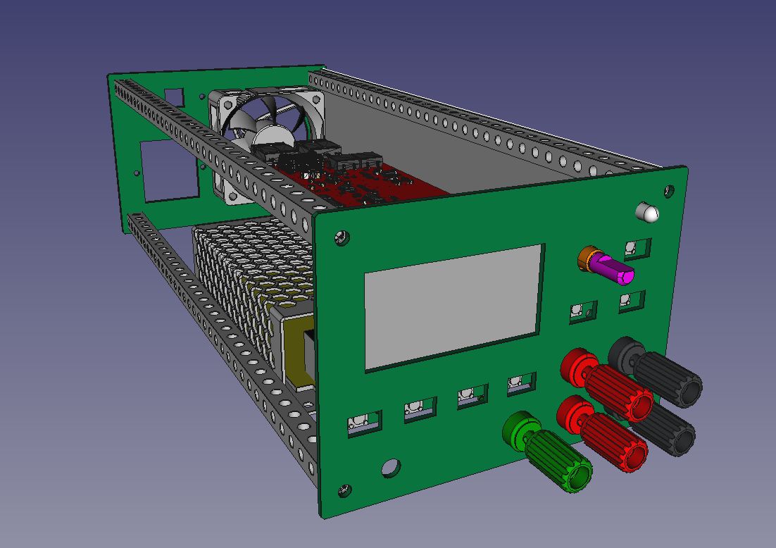
Enclosure
Here is a first pass at
an enclosure and front panel for a single channel PS-Load MkII.
- 24V 4A using 100W
MeanWell supply
- 2U (3.5") x 4.75" x
11.2" enclosure using Gobilda rails
- New front panel
board with 2.42" OLED display and Arduino Nano Every
- Heat sink, AC In,
bottom plate, are not shown
A first pass
front panel. Haven't decided what all the buttons do. Since this
is not a touch panel, I need the buttons to be flexible. The 4
buttons below the OLED could be soft keys, with labels on the
OLED.
Here is the proposed CPU board with 2.4" OLED.
And the Nano Every on the back.
Here is the prototype for PS-Load MKII, next to the original.
Processor is the Nano Every. The basic controls for setting
voltage and measuring voltage and current are working. I'm liking
the big new 2.42" OLED displays. Even the default 5x7 font is
visible from a distance.
Love affair with Nano
Every and Teensy 3.2 has ended :-(
Now that the Covid parts shortage dust has settled, it's time for
a new processor. My new fave low-end processor is the Adafruit
Itsy Bitsy M0. It has lots of I/O, a SAMD21 48MHZ ARM processor,
lots of memory, and a nice 12 bit ADC. And it costs the same $12
as the Nano-Every, whose price has increased. It has
upgrades via the Adafruit Feather product line. I picked the
Itsy-Bitsy because it is smaller and has more I/O than the
Feather, and costs less. It supports MicroPython for you Python
people.
I have one talking to the OLED, and have the 1mS interrupt
working. Next to move it to the PS-Load proto.
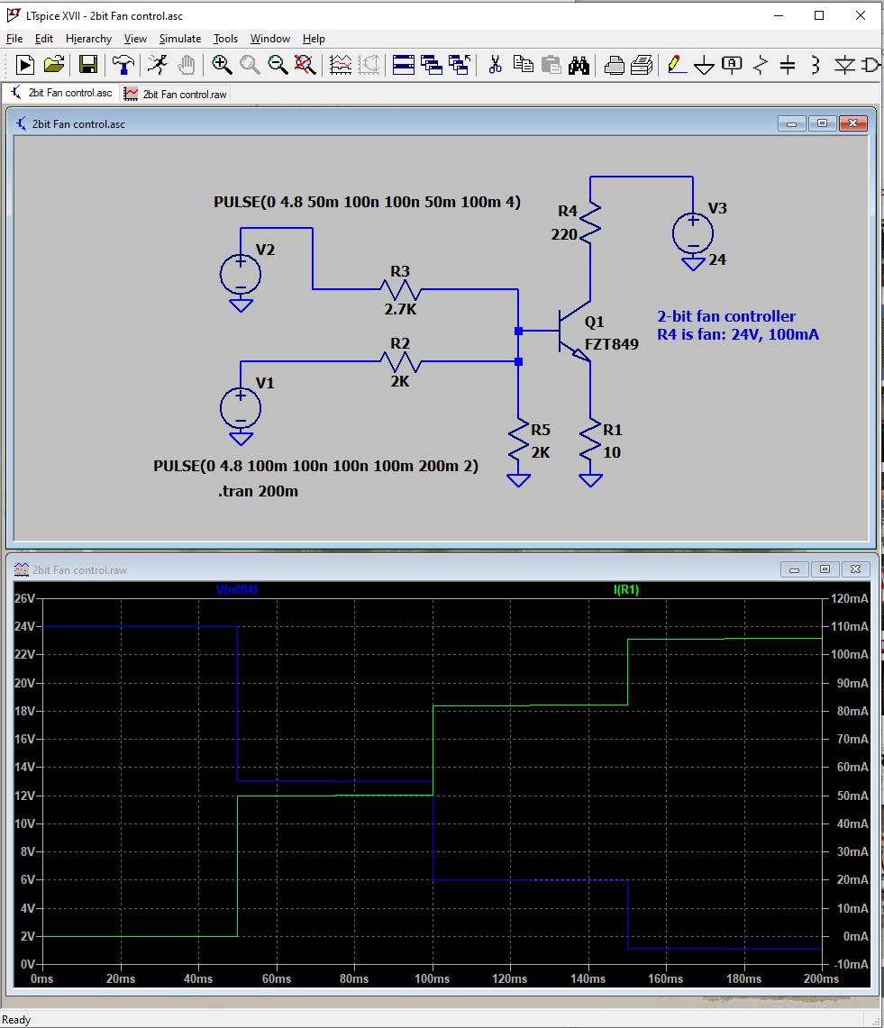
2-bit fan controller
Recognizing that many
projects I do need a fan controller, and my separate fan control
board is a bit over-complicated, here is my latest thinking.
DC brushless fans can be driven by a varying DC voltage or by a
pulsating DC. Pulsating DC can cause acoustic and electrical
noise. I thought I'd try using a simple DC current drive. It supports 3 levels of fan
speed plus off, and uses two isolated 5V control bits, which
PS-Load has plenty of. It uses a simple power transistor as a
crude voltage-to-current controller. I simulated and tested it and
it works well. It will work with most fans up to a few watts: 12,
24 or 48V. Just change the 10 ohm resistor to increase or decrease
the fan current. The transistor can be any NPN power device
capable of dissipating about 1W: TO-220, SOT-223 or D-PAK.
The output across the fan should be filtered by about a 22-100uF
cap since fan motors draw pulsating currents. Since it is
controlled by the CPU, it can be operated in a closed loop by the
CPU monitoring the heat-sink temperature, or open loop, by
estimating temperature rise based on dissipated power. In
the case of PS-Load, the firmware knows the output V, Power supply
V, and output current, so it can calculate the FETs power
dissipation. This, plus the heat sink thermal resistance can be
used to estimate temp. rise of the FETs. Then adjust the fan speed
accordingly. Ideally you would also know
the ambient temperature, but since this is a laboratory
instrument, a small range of ambient temperatures can be
assumed. Not true if you need to operate from a wide range of
temperatures. Saves a temperature sensor and its wiring
and mounting.
The
Blog for this project
The
DIY-SMU project
Dave's Home Page
Last Updated:
7/25/2024